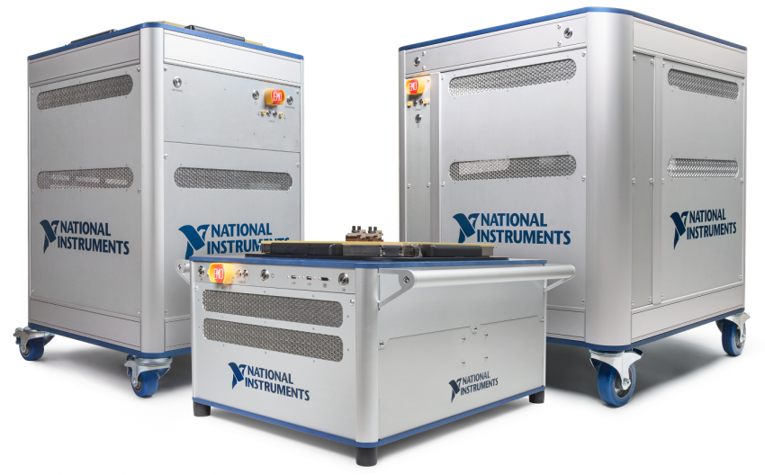
Multi-Site Wafer Level Testing on NI STS
Problem
When a company purchases an NI STS it is shipped “blank”, with only the necessary development environments installed. In order to use the STS for wafer level testing you need to develop, approve and release your test sequences. A bit like when you first open your new laptop, before you can start writing an email you need to download some stuff first.
As this was the first product to be tested using the NI STS there was the added pressure of investigating if it offered better efficiency that their current pool of testers. This includes sequence development time, sequence validation, total test time and reliability.
Result
In co-operation with the test engineering department we developed a series of drag and drop style tests to allow quick and flexible configuration of test sequences for the wafer level testing of numerous device types. This flexibility adds a long term benefit to the department as it can encompass whole product ranges, expand to future developments and is fully open to everyone.
For future products the benefits will be even greater, as all code is already verified for memory leaks, error handling etc. and the basis template already includes all the basic tests required by the QA department.
By making everything as generic as possible, we not only solved the problem but in doing so added great value to the department.
Solution
To find the right results there were 2 problems that need to be solved. The first was obvious, we needed to be able to quickly and easily create test sequences for a variety of devices. The second issue was that not all the test engineers were LabVIEW programmers. We needed to find a way to limit their exposure to the programming side and just allow them to create tests, not program them.
The first step was to use LabVIEW to develop the individual tests, this allowed us to have the flexibility to test the hardware as well as find optimal architecture for the software. Each test was developed, debugged and optimised in a lab environment to avoid unnecessary time in the actual test area (this was a clean room environment and wasn’t the most comfortable place to work!)
We adopted a “one VI, one job” approach in that single VI did exactly one task. This allows maximum re-use of the code and makes everything much clearer. For most tests there was just a single layer of VIs, no huge complicated hierarchy or dependencies to manage.
During this development we asked other departments to analyse some of the data – using various statistical methods – and also held code reviews to both check for mistakes and explain the operation. This proved quite interesting as there were often 2 or 3 ways of doing the same test, with different people arguing for each method. In some cases we developed 2 ways and tested for the quickest, the first idea was not always the best.
As the STS hardware and the TSM software were relatively new products, we were in constant close contact with NI regarding issues, bugs and potential improvements. Between ourselves, NI and our customer we successfully implemented a test sequence that enabled multisite wafer level testing of LNAs and dramatically reduced the total test time for the whole wafer.
With the solution we chose, it allows the hardware to be used on other products simply and quickly. In the event of a system issue, it is so quick to change the software on an STS that it would be feasible to take a system from another production line to reduce the downtime.
For more information on wafer level testing, the NI STS or to see how we can help you, please contact us
To read our alternative review of the NI STS, see here
This project is part of our Semiconductor division
Technologies:
Categories:
Tags:
Our Portfolio